
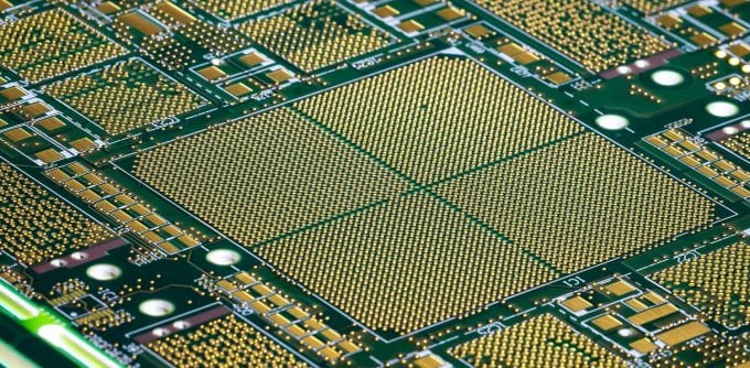
High-Density Interconnection printed circuit boards or HDI PCB is a type of technology that started getting popular during the 20th century and being used anywhere where the higher density could benefit. Any device that would require more processing power (such as a smartphone) and reduced size and weight, an HDI PCB is always used.
The reason why this type of PCB can fit in so many components is that it has multiple layers when compared to a conventional board. With the use of metalization and laser drilling, you can add an inner layer line and an outer layer line. This is what made this type of board so popular during the 20th century.
Keep in mind, not every single HDI PCB gets two-layered. If you want to have a higher-tech grade PCB then you will have to stack the layers while most ordinary HDIs are just laminated one time. Two or more layers of technology is a bit more expensive and is done only if the highest quality of boards is required.
However, even with the access with such an advanced type of PCB, designers still have a hard time thinking of a good PCB layout. An expert in PCB layouts has to make several difficult decisions which will ultimately lead to the final specifications of the board. This part of the process gets even more complicated if the PCB needs to be as high quality as possible. It will probably be used in medical devices, military vehicles such as tanks, tactical SUVs, helicopters and so on. It could also be used for airliners which means it needs to be designed properly to ensure the highest level of safety for its future passengers.
In other words, for the highest possible performance, the design layout needs to be developed by an experienced expert.
To achieve the best possible layout, the designers must implement the general engineering practice known as Design for Manufacturability which is also known as DFM. It is a practice that pushes the design to be easily manufacturable. The easier it is to manufacture, the lesser chances of future errors, problems, and the devices will be of overall higher quality.
Still, even when following the most popular engineering practices to ease your work, making the most efficient HDI PCB design is still difficult. Fortunately for you, we have made this list of design tips to help you. If you want to know more about the benefits and features of High-Density Interconnection printed circuit boards, you should definitely read more about it.
Pick the right via type
Naturally, if you are planning the layout of the PCB, you will also have to consider what type of visa you will use. Via is a pad with thru-holes (plated holes) that allow the copper tracks to get from one layer of the board to another. Since some boards can go anywhere between one to eight layers and some special PCBs can have up to a hundred layers, having these plated holes are essential.
To properly send information through the holes, however, you will need the right type of via. The via you choose in the end will influence the final production costs, the manufacturing time and the kind of equipment that will be used during the process.
So, when choosing whether you are going to use a neap pad, dogbone or a via-in-pad, keep in mind just how much impact it will have on the cost of the manufacturing process. Sure, having the highest quality of materials is always preferred, but you do not want to push the costs too high, right?
Component optimization
For most conventional boards, optimizing the components is not a very important step in the layout design process, but when it comes to HDI PCBs, it is very important that every component is carefully selected for the best performance possible. The design of your HDI and the components you choose will affect things such as sizes and types of stackup and influence the trace widths and locations of drill holes.
Naturally, when choosing the components for the layout, the first thing you consider is the capability of their performance, but you will also have to consider their availability. There’s no point in picking a part that will boost the performance of the PCB by just a small margin while its availability is almost zero. Finding this kind of component will be impossible and expensive. And if the manufacturing plant does manage to find a supply of such a component, if the supply ends, finding a substitute will increase both the time and cost of the manufacturing process.
This is why we recommend to every PCB designer to avoid this kind of design.
Keep Electromagnetic Interference (EMI) to its minimum
You probably already know just how much electromagnetic interference can impact the signal quality of the board. This is why we recommend that you avoid spacing the components so closely when drawing the layout of the PCB. It is also important that you place the vias symmetrically. If you do not, the chances that the board might bend or warp are very high. All that uneven stress can cause the heat of the components to ramp up which is never good when it comes to HDI PCBs.
Use shorter trace lengths
The fact that HDI PCBs can have much smaller trace widths to ultimately increase the number of signals that can be sent through the board is a great advantage over conventional PCBs. However, with such an advantage, there is always a negative effect that comes with it. The length of the traces will need to be kept shorter than usual because it might affect the integrity of the signal. We recommend that you use the shortest possible trace lengths when working on the layout design of an HDI PCB.
To help you understand what all of these tips aim for, we are going to sum everything up in just one sentence. do everything in your power to increase the performance of the board, but also reduce the cost of the manufacturing process. That is what a good PCB designer always does.


